Call us now

 Send Inquiry
Dry Film Photoresist
Price 1 USD ($)/ Container
MOQ : 1 Metric Ton
Dry Film Photoresist Specification
- Type
- Dry Film
- Material
- Photosensitive Polymer
- Tensile Strength
- >50 MPa
- Working Temperature
- 15C - 25C
- Density
- 1.2 Gram per cubic centimeter(g/cm3)
- Length
- 10 meters (standard)
- Width
- 30 cm, 32 cm (standard)
- Thickness
- 30-50 micron
- Transparency
- High Transparency
- Hardness
- Flexible
- Size
- Customizable Roll Size
- Color
- Blue
- Handling Precautions
- Avoid direct contact and dust contamination
- Exposure Wavelength
- 350-400 nm
- Storage Conditions
- Store in cool and dry place away from sunlight
- Adhesion
- Strong adhesion to copper-clad laminates
- Surface Finish
- Smooth and Glossy
- Peel Strength
- >1.0 N/cm
- Curing Time
- 30-60 seconds (varies with UV intensity)
- Shelf Life
- 12 Months
- Environmental Compliance
- RoHS Compliant
- Release Liner
- PET Film
- Photo Sensitivity
- High, ideal for fine lines and patterns
- Application
- PCB Manufacturing, Pattern Plating, Etching
- Developer
- Aqueous Alkaline Solution
- Solvent Resistance
- High
- Etching Resistance
- Excellent
Dry Film Photoresist Trade Information
- Minimum Order Quantity
- 1 Metric Ton
- Certifications
- ISO 14001 ,OHSAS18000 ,ISO 9001
About Dry Film Photoresist
For high return and great efficiency, our Dry Film Photoresist is perfect for a wide range of plating and drawing applications. Following utilizing dry cover, stripping scope and gangs wide introduction, this concoction is acknowledged for offering incredible adaptation. Likewise, Dry Film Photoresist can be utilized specifically on move laminators. Our offered concoction is likewise utilized for printed circuit panel. In addition, our offered photoresist is special decision for picture exchanging process. Moreover, this photoresist is impervious to water and UV.The worldwide pattern of electronic correspondence items is toward exceptionally exact and thin plan. The innovation and nature of fabricate is essential as to ensure our Dry Film Photoresist is the definitive critical material to the manufacturing of correspondence devices. Our company has effectively centered on the change of assembling innovation for quite a while, and participated to deliberately create different photoresists for various assembling process. Our product has certifications of TOSHMS, ISO and OHSAS.
Features:
- Brilliant time span of usability
- Safe to utilize
- Can be effectively used
Exceptional Precision and Durability
Engineered for state-of-the-art PCB processes, this dry film photoresist ensures fine line definition and robust chemical resistance. Its flexible and transparent structure facilitates easy handling while maintaining strong adhesion and a glossy surface, resulting in highly reliable components even under demanding conditions.
Easy Processing and Consistent Results
With a 30-60 second curing time under 350-400 nm UV exposure, this photoresist enables efficient throughput in manufacturing. Its PET release liner ensures clean application, and compatibility with aqueous alkaline solutions provides safer and more predictable development results.
Safe Storage and Versatile Applications
Maintain optimal performance by storing the film in cool, dry environments away from sunlight. Its RoHS-compliance and customizable dimensions make it suitable for various applications, including professional PCB manufacturing, pattern plating, and precision etching across diverse production scales.
FAQs of Dry Film Photoresist:
Q: How do I apply the dry film photoresist to a copper-clad laminate?
A: Clean the copper surface thoroughly to remove dust and oils, then carefully laminate the dry film photoresist onto the surface. Use a laminator or press under recommended temperature and pressure, ensuring the PET release liner is left intact until after lamination.Q: What benefits does this dry film photoresist offer for fine-line PCB manufacturing?
A: The high photosensitivity, strong adhesion, and smooth glossy surface facilitate accurate reproduction of fine lines and patterns. Its excellent etching resistance and high transparency enable consistent results for intricate PCB or pattern plating applications.Q: Where and how should I store the dry film photoresist for optimal shelf life?
A: Store the film in a cool, dry place, away from exposure to sunlight. Ideal storage temperatures are between 15C and 25C. Following these guidelines preserves photosensitivity and extends its shelf life up to 12 months.Q: What is the recommended process for developing and curing the photoresist after exposure?
A: After exposure to UV light (350-400 nm) for 30-60 seconds, immerse the laminated panel in an aqueous alkaline solution to develop the image. Rinse thoroughly with water after developing to remove any residue. Avoid direct contact and keep the surface dust-free during processing.Q: What are the handling precautions I need to observe?
A: Wear gloves and handle the film in a clean environment to avoid contamination. Avoid direct contact with the photosensitive surface and shield the film from dust to ensure a defect-free final pattern.Q: When should I replace the dry film photoresist?
A: Use the film within 12 months of manufacture for optimal effectiveness. Discard it if you notice reduced adhesion or compromised pattern transfer, which can result from improper storage or expired material.Q: What customization options are available for the films size and thickness?
A: The dry film photoresist is supplied in standard widths of 30 cm and 32 cm, lengths of 10 meters, and thicknesses between 30-50 microns. Custom roll sizes can be ordered directly from the Taiwan-based distributor or manufacturer to suit specific application requirements.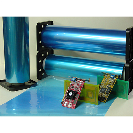
Tell us about your requirement

Price:
Quantity
Select Unit
- 50
- 100
- 200
- 250
- 500
- 1000+
Additional detail
Mobile number
Email

GREAT EASTERN RESINS INDUSTRIAL CO., LTD.


Ms Irene Chen
(Marketing Specialist)
Mobile : +88623587676
No.35, 34th Road, Industrial Park, 407, R.O.C., Taichung - 40768, Taiwan

Quick Link
Developed and Managed by Infocom Network Private Limited.
